Small component pitch – meaning very tight spacing between pads, traces, or terminations – creates a perfect storm of electrical, mechanical, and contamination-driven risks. It’s one of the most important component layout factors in modern electronics because shrinking pitch amplifies every weakness in the assembly process and the operating environment.
When two conductors sit close together – traces, pads, vias, or terminations – the small gap between them can trap and hold moisture from the environment. This moisture does not behave like free water; it forms:
• A thin absorbed water layer on surfaces
• A micro-humidity pocket that exchanges moisture slowly with the surrounding air
• A conductive film when ions are present
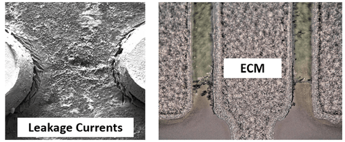
Tiny chip capacitors and bottom-terminated components have narrow gaps that behave like capillaries. These gaps can pull moisture in, especially when ionic contamination is present. Since there is no airflow, the moisture can remain and slowly evaporate.
The combination of moisture and ionic contamination increases electrical stress. Tighter spacing is a major cause of short-circuit failures.
Best practice is to select a no-clean flux with proven SIR performance. Cleaning the assembly after soldering removes sources of ionic contamination. When cleaning, confirm that wash chemistry, cleaning machine, and wash parameters are defined to achieve no residue under component terminations. Use SIR test boards representative of production hardware to verify cleanliness.